
Identify the CORRECT energy band diagram for Silicon doped with Arsenic. Here CB, VB, E$_D$ and E$_F$ are conduction band, valence band, impurity level and Fermi level, respectively.
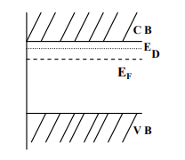
Energy Band Diagram for Silicon Doped with Arsenic
This question requires identifying the correct energy band diagram for Silicon (Si) doped with Arsenic (As).
Understanding Semiconductor Doping
Silicon is a Group IV element. Arsenic is a Group V element. When Arsenic is added as an impurity to Silicon, each Arsenic atom replaces a Silicon atom and contributes one extra valence electron that is not needed for bonding.
- This makes the semiconductor n-type, where electrons are the majority charge carriers.
- The extra electrons from Arsenic atoms create donor energy levels (denoted as ED).
- These donor levels are located close to the conduction band (CB).
- In an n-type semiconductor, the Fermi level (EF) shifts from the middle towards the conduction band. It lies between the donor level (ED) and the conduction band (CB).
Analyzing the Energy Band Diagram
Based on the principles of n-type doping:
- The diagram must show the Conduction Band (CB) and Valence Band (VB) separated by the band gap.
- A discrete donor energy level (ED) must be present just below the CB.
- The Fermi level (EF) must be located between ED and CB.
Comparing these requirements with the provided options:
- Option B (the second image) accurately depicts this configuration: ED is close to CB, and EF lies between ED and CB.
Conclusion
Therefore, the correct energy band diagram for Silicon doped with Arsenic corresponds to the configuration shown in Option B.
Important Questions from Band Theory Effective Mass Holes
- For the energy dispersion of an electron in a one-dimensional solid $E(k) = E_0 - 2\gamma \cos(ka)$, the ratio of the effective mass of the electron in the solid to the free electron mass ($m_e$) at $k = 0$ is $R_0$. Taking $\gamma = 0.5 \text{ eV}$ and $a = 0.5 \text{ nm}$, the value of $R_0$ (rounded off to two decimal place) is _____
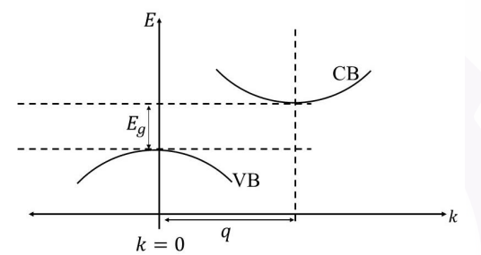
($\hbar = 1.054 \times 10^{-34} \text{ J.s}$, $m_e = 9.1 \times 10^{-31} \text{ kg}$, electron charge $= 1.6 \times 10^{-19} \text{ C}$) The dispersion ($E(k)$) of the conduction band (CB) and valence band (VB) for a semiconductor are shown schematically in the figure. Considering the possibility of an electron making a transition from the bottom of the CB to the top of the VB, which of the following options is/are correct?
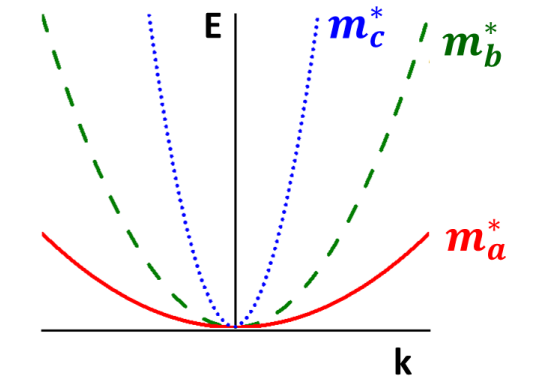
For nonrelativistic electrons in a solid, different energy dispersion relations (with effective masses $m_a^*$, $m_b^*$, and $m_c^*$) are schematically shown in the plots. Which one of the following options is CORRECT?
The temperature dependence of the electrical conductivity ($\sigma$) of three intrinsic semiconductors A, B and C is shown in figure.
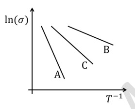
Let $E_A$, $E_B$ and $E_C$ be the bandgaps of A, B and C, respectively. Which one of the following relations is correct?- The energy dispersion for electrons in one dimensional lattice with lattice parameter $a$ is given by $E(k) = E_0 - \frac{1}{2} W \cos ka$, where $W$ and $E_0$ are constants. The effective mass of the electron near the bottom of the band is


