
(A) Diodes can be used for rectifying an ac voltage.
(B) For semiconductors, band gap energy $E_g > 3 \text{ eV}$.
(C) By changing the external applied voltage, junction barriers can be changed.
(D) p-n junction is the 'key' to all semiconductor devices.
Choose the correct answer from the options given below:
Analyzing Statements on Electronic Devices
This question asks us to evaluate the correctness of four statements related to fundamental concepts in electronic devices and semiconductor physics.
Statement (A): Diodes and AC Voltage Rectification
Statement (A) claims that diodes can be used for rectifying an AC voltage. This is correct. A diode is a two-terminal electronic component that conducts current primarily in one direction. This property makes it ideal for rectification, the process of converting alternating current (AC) into direct current (DC). By allowing current to flow during only one half-cycle of the AC input, a diode effectively blocks the other half-cycle, resulting in a pulsating DC output.
Statement (B): Semiconductor Band Gap Energy
Statement (B) suggests that for semiconductors, the band gap energy ($E_g$) is greater than $3 \text{ eV}$. This statement is generally incorrect. While some wide-bandgap materials used in specific applications might have energies exceeding $3 \text{ eV}$ (and are often classified closer to insulators), common semiconductors like Silicon (Si) have a band gap of approximately $E_g \approx 1.1 \text{ eV}$, and Germanium (Ge) has $E_g \approx 0.7 \text{ eV}$. Gallium Arsenide (GaAs), another important semiconductor, has $E_g \approx 1.4 \text{ eV}$. Materials with band gaps significantly larger than $3 \text{ eV}$ are typically considered insulators.
Statement (C): Changing Junction Barriers with Applied Voltage
Statement (C) states that junction barriers can be changed by altering the external applied voltage. This is a core principle of semiconductor device operation, particularly for the p-n junction. When a voltage is applied across a p-n junction (forward bias or reverse bias), it modifies the width of the depletion region and the height of the potential energy barrier at the junction. Forward bias reduces the barrier height, allowing current flow, while reverse bias increases the barrier height, significantly reducing current flow.
Statement (D): The p-n Junction as a Key Component
Statement (D) posits that the p-n junction is the 'key' to all semiconductor devices. This highlights the fundamental importance of the p-n junction. Essential semiconductor devices like diodes, bipolar junction transistors (BJTs), field-effect transistors (FETs), and integrated circuits all rely on the unique electrical characteristics created by joining p-type and n-type semiconductor materials. Understanding the behavior of the p-n junction is crucial for designing and analyzing these devices.
Conclusion on Correct Statements
Based on the analysis:
- Statement (A) is True.
- Statement (B) is False.
- Statement (C) is True.
- Statement (D) is True.
Therefore, the correct combination of true statements includes (A), (C), and (D).
Important Questions from Semiconductor and Electronic Devices
Silicon can be doped using one of the following elements as dopant:
(A) Arsenic
(B) Indium
(C) Phosphorus
(D) BoronTo get an n-type semiconductor, the dopants that can be used are:
Let iE, iC, and iB represent the emitter current, collector current, and the base current respectively in a transistor. Choose the correct statement:
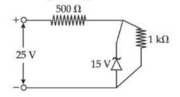
A Zener diode is used in a voltage regulator circuit as shown below. Its breakdown voltage is 15 V. What is the current flowing through the Zener diode?
Choose the correct experimental circuit arrangement for studying V-I characteristics of a p-n junction diode in forward bias:
During the p-n junction formation, when an electron diffuses from n → p, it leaves behind an:


