
Which of the following statements are correct? A. In semiconductor diodes, carriers are generated by photo-excitation. B. When the photo diode is illuminated with light with energy (E) > Energy gap (Eg) of the semiconductor, then electron-hole pairs are generated. C. Photovoltaic devices convert electricity into optical radiation. D. Photodiode can be used as a photodetector to detect optical signal. E. Zener diode specification should be taken as per the required output voltage. Choose the correct answer from the following options given below:
A, B, D and E only
Understanding Semiconductor Devices: Diodes, Photodiodes, and Zener Diodes
Let's analyze each statement provided in the question to determine its correctness in the context of semiconductor devices.
Statement A: In semiconductor diodes, carriers are generated by photo-excitation.
This statement suggests that photo-excitation is a mechanism for generating charge carriers in semiconductor diodes. While thermal generation and generation due to doping are common in all semiconductor diodes, photo-excitation is specifically the principle behind light-sensitive semiconductor devices like photodiodes and solar cells, which are types of semiconductor diodes. When light falls on a semiconductor with sufficient energy, it can excite electrons, creating electron-hole pairs. Therefore, photo-excitation is indeed a mechanism for carrier generation in certain semiconductor diodes, making this statement considered correct in this context.
Statement B: When the photo diode is illuminated with light with energy (E) > Energy gap (Eg) of the semiconductor, then electron-hole pairs are generated.
This statement describes the fundamental principle of photo-excitation in semiconductors. For a photon of light to generate an electron-hole pair, its energy (E) must be greater than or equal to the energy band gap (\(E_g\)) of the semiconductor material. If \(E \ge E_g\), the photon has enough energy to excite an electron from the valence band to the conduction band, leaving a hole in the valence band. This creates a mobile electron-hole pair. This statement is correct.
\(E \ge E_g\)
where:
- \(E\) is the energy of the incident light photon.
- \(E_g\) is the energy band gap of the semiconductor material.
Statement C: Photovoltaic devices convert electricity into optical radiation.
Photovoltaic devices, such as solar cells, operate on the principle of the photovoltaic effect. They convert energy from optical radiation (light) into electrical energy (electricity). The reverse process, converting electrical energy into optical radiation, is performed by devices like Light Emitting Diodes (LEDs). Therefore, this statement is incorrect.
Statement D: Photodiode can be used as a photodetector to detect optical signal.
A photodiode is designed specifically to detect light (optical signals). When light with energy greater than the band gap strikes the photodiode's PN junction, it generates electron-hole pairs. This generation causes a change in current (when reverse biased) or voltage (when open circuit/photovoltaic mode), which can be measured and used to detect the presence and intensity of the optical signal. This is the primary function of a photodiode. This statement is correct.
Statement E: Zener diode specification should be taken as per the required output voltage.
Zener diodes are primarily used as voltage regulators. When a Zener diode is reverse-biased and the voltage across it reaches its Zener voltage (\(V_z\)), it enters a breakdown region where the voltage across the diode remains nearly constant, even if the current through it changes significantly. In voltage regulation circuits, the Zener diode is chosen such that its specified Zener voltage (\(V_z\)) matches the desired regulated output voltage. Therefore, the Zener diode specification, particularly its Zener voltage, is selected based on the required output voltage. This statement is correct.
Summary of Statements
Based on the analysis:
- Statement A: Correct (Photo-excitation is a carrier generation mechanism in semiconductor diodes, especially photodiodes).
- Statement B: Correct (Light energy > Band gap generates electron-hole pairs).
- Statement C: Incorrect (Photovoltaic devices convert light to electricity, not vice versa).
- Statement D: Correct (Photodiode is used as a photodetector).
- Statement E: Correct (Zener diode chosen based on required voltage regulation).
The correct statements are A, B, D, and E.
| Statement | Analysis | Correctness |
|---|---|---|
| A | Carrier generation by photo-excitation in semiconductor diodes. | Correct |
| B | E > Eg for electron-hole pair generation by light. | Correct |
| C | Photovoltaic devices convert electricity to optical radiation. | Incorrect |
| D | Photodiode used as a photodetector. | Correct |
| E | Zener diode spec based on required output voltage. | Correct |
Conclusion on Correct Statements
Based on our evaluation, statements A, B, D, and E are correct.
Revision Table: Semiconductor Device Principles
| Device/Concept | Principle | Key Function |
|---|---|---|
| Photodiode | Photo-excitation (\(E \ge E_g\)) generates carriers. | Detecting optical signals (photodetector). |
| Photovoltaic Device (e.g., Solar Cell) | Photovoltaic effect: Light energy converted to electrical energy. | Power generation from light. |
| Light Emitting Diode (LED) | Electroluminescence: Electrical energy converted to light energy. | Emitting optical radiation. |
| Zener Diode | Zener breakdown (reverse bias). | Voltage regulation. |
| Carrier Generation | Creation of mobile electrons and holes in a semiconductor (can be thermal, optical, or due to high electric field). | Fundamental process for device operation. |
Additional Information on Semiconductor Devices
Semiconductor devices like diodes are fundamental building blocks in electronics. Their properties are based on the behavior of charge carriers (electrons and holes) within semiconductor materials like silicon or germanium, often modified by doping.
- PN Junction: The interface between a p-type and an n-type semiconductor is called a PN junction. This junction forms the basis of most diodes, including standard diodes, photodiodes, and Zener diodes. The behavior of carriers across this junction under different biases (forward or reverse) is key to their functionality.
- Carrier Generation Mechanisms:
- Thermal Generation: At any temperature above absolute zero, thermal energy can break covalent bonds, creating electron-hole pairs. This happens in all semiconductors.
- Photo-excitation: As discussed, photons with sufficient energy can generate electron-hole pairs. This is utilized in photodiodes and solar cells.
- Impact Ionization/Zener Breakdown: In a strong electric field (typical in reverse breakdown), carriers can gain enough energy to knock out valence electrons, creating new electron-hole pairs. This is the mechanism behind Zener breakdown in Zener diodes and avalanche breakdown.
- Photodiode Operation: Photodiodes are typically operated under reverse bias. Incident light generates carriers near the PN junction, and the electric field separates these carriers, causing a reverse current proportional to the light intensity.
- Zener Diode Operation: Zener diodes are designed with a heavily doped junction that exhibits a sharp breakdown voltage (\(V_z\)) in reverse bias. This stable voltage makes them ideal for regulating voltage levels in circuits.
Understanding these principles is crucial for analyzing and designing electronic circuits using semiconductor components.
Important Questions from Semiconductor and Electronic Devices
Silicon can be doped using one of the following elements as dopant:
(A) Arsenic
(B) Indium
(C) Phosphorus
(D) BoronTo get an n-type semiconductor, the dopants that can be used are:
Let iE, iC, and iB represent the emitter current, collector current, and the base current respectively in a transistor. Choose the correct statement:
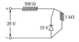
A Zener diode is used in a voltage regulator circuit as shown below. Its breakdown voltage is 15 V. What is the current flowing through the Zener diode?
Choose the correct experimental circuit arrangement for studying V-I characteristics of a p-n junction diode in forward bias:
During the p-n junction formation, when an electron diffuses from n → p, it leaves behind an:


