NMOS Transistor Temperature Effects on I-V Characteristics
This question explores how changes in temperature affect the current-voltage (I-V) characteristics of an NMOS (N-channel Metal-Oxide-Semiconductor) transistor, specifically focusing on the ON-current ($I_{ON}$) and the OFF-current ($I_{OFF}$). Understanding these effects is crucial for designing reliable electronic circuits.
Understanding Temperature Impact on NMOS Parameters
Temperature significantly influences several fundamental parameters of a semiconductor device like the NMOS transistor:
- Carrier Mobility ($\mu$): In silicon, as temperature increases, lattice vibrations (phonons) become more energetic. This leads to increased scattering of charge carriers (electrons in NMOS) as they move through the silicon lattice. Consequently, the carrier mobility, which measures how easily carriers move, decreases with rising temperature. Mathematically, mobility $\mu \propto T^{-\n}$ where $T$ is temperature and $n$ is a positive exponent (typically around 1.5 to 2.5 for lattice scattering).
- Threshold Voltage ($V_{th}$): The threshold voltage is the minimum gate-to-source voltage ($V_{GS}$) required to turn the transistor ON. For NMOS transistors, the threshold voltage generally decreases as temperature increases. This is because the Fermi level position relative to the intrinsic Fermi level shifts with temperature, reducing the voltage needed to create the inversion layer.
- Subthreshold Swing (S): The subthreshold swing indicates how sharply the transistor transitions from the OFF state to the ON state. It is defined as $S = \frac{d V_{GS}}{d (\log_{10} I_D)}$. A smaller $S$ means a sharper turn-on. Increasing temperature generally improves (decreases) the subthreshold swing, making the transition faster.
Analyzing ON-Current ($I_{ON}$) Variation
The ON-current ($I_{ON}$) represents the current flowing through the transistor when it is fully turned ON (i.e., when $V_{GS}$ is significantly greater than $V_{th}$). The drain current ($I_D$) in the saturation region can be approximated as:
$ I_D \approx \frac{1}{2} \mu C_{ox} \frac{W}{L} (V_{GS} - V_{th})^2 $
Where:
- $\mu$ is the carrier mobility
- $C_{ox}$ is the gate oxide capacitance per unit area
- $W/L$ is the aspect ratio of the transistor
- $V_{GS}$ is the gate-to-source voltage
- $V_{th}$ is the threshold voltage
From the equation, $I_{ON}$ is directly proportional to mobility ($\mu$). Since mobility decreases significantly with increasing temperature due to lattice scattering, the ON-current ($I_{ON}$) tends to decrease.
While the threshold voltage ($V_{th}$) also decreases with temperature (which would tend to slightly increase $I_{ON}$), the effect of reduced mobility is typically dominant, leading to an overall decrease in $I_{ON}$.
Analyzing OFF-Current ($I_{OFF}$) Variation
The OFF-current ($I_{OFF}$) is the small leakage current that flows when the transistor is supposed to be OFF (i.e., $V_{GS} < V_{th}$). This current has several components, primarily:
- Reverse-biased junction leakage current (between drain/source and substrate).
- Band-to-Band Tunneling (BTBT) related leakage.
- Subthreshold leakage current, which is exponentially dependent on $V_{GS}$ and $V_{th}$.
These leakage mechanisms are highly sensitive to temperature.
- The reverse saturation current of the PN junctions increases exponentially with temperature.
- Carrier generation rates within the depletion region also increase significantly with temperature.
- Furthermore, the decrease in $V_{th}$ with temperature means that for a fixed $V_{GS}$, the overdrive $(V_{GS} - V_{th})$ becomes less negative (or more positive if $V_{GS}$ was close to $V_{th}$), slightly increasing the subthreshold leakage.
Due to these factors, the OFF-current ($I_{OFF}$) increases significantly as the temperature rises.
Summary of Temperature Effects
In summary, increasing the temperature in an NMOS transistor leads to:
- A decrease in carrier mobility ($\mu$).
- A decrease in threshold voltage ($V_{th}$).
- A dominant decrease in the ON-current ($I_{ON}$) primarily due to reduced mobility.
- A significant increase in the OFF-current ($I_{OFF}$) due to increased junction leakage and subthreshold conduction mechanisms.
Therefore, the effect of increasing temperature is that $I_{ON}$ will decrease and $I_{OFF}$ will increase.
Important Questions from MOSFET
An n-channel MOSFET is connected as shown in the Figure.
Assume $V_{TH} = 1\text{ V}$, $V_{DD} = 5\text{ V}$, and $\mu C_{ox}\left(\frac{W}{L}\right) = 2\text{ mA V}^{-2}$ and neglect channel length modulation effects.
The gate voltage ($V_G$) of the n-channel MOSFET (in Volt) is __.
(rounded off to two decimal places)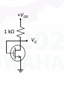
- A semiconductor uses P-type substrates with $N_A = 5 \times 10^{15}cm^{-3}$ in an n-MOS device having depletion region width of 0.415 $\mu$m. What is the depletion charge in magnitude?
- MOSFETs exhibit a non-linear relationship between input voltage and output current due to the device construction. The non-linear relationship is connected through the device parameter 'K'. Calculate 'K' for a specific MOSFET operating with an input voltage of 6 V and output current of 10 mA. The Threshold voltage of the chosen MOSFET is 4 V.
- Given below are two statements: one is labelled as Assertion (a) and the other is labelled as Reason (r).
Assertion (a): In a ratioless logic, the transistors can be of minimum size.
Reason (r): In a ratioless logic, the logic levels are not dependent upon the relative device size. MOSFET can be used as a ____________.