Assertion (a): In a ratioless logic, the transistors can be of minimum size.
Reason (r): In a ratioless logic, the logic levels are not dependent upon the relative device size.
Ratioless Logic: Transistor Size and Logic Levels Explained
This question explores the characteristics of ratioless logic circuits, specifically focusing on the size of transistors used and the dependency of logic levels on device sizes.
Understanding Ratioless Logic
In digital circuit design, particularly in CMOS technology, logic gates are often designed using transistors. Traditionally, the ratio of the sizes (width-to-length ratio) of the pull-up and pull-down transistors was critical for ensuring proper logic levels (a strong '0' and a strong '1'). However, ratioless logic designs are different.
Ratioless logic circuits aim to achieve correct logic level operation without strictly relying on the precise ratio between the sizes of the transistors involved. This often involves using active loads or dynamic operation principles.
Analysis of Assertion (a)
Assertion (a): In a ratioless logic, the transistors can be of minimum size.
This statement is correct. Because ratioless logic designs do not depend on specific size ratios for their functionality, designers have the flexibility to use transistors at or near their minimum allowable sizes. This choice can lead to benefits like reduced chip area and potentially lower power consumption, provided the circuit still operates correctly.
Analysis of Reason (r)
Reason (r): In a ratioless logic, the logic levels are not dependent upon the relative device size.
This statement is also correct and provides the fundamental reason behind the characteristic mentioned in Assertion (a). In ratioless logic families (like certain dynamic logic circuits), the stability and definition of the logic high and logic low voltage levels are maintained through mechanisms other than just the sizing ratio of the pull-up to pull-down transistors. For instance, a precharge phase might establish a known level, or active loads might ensure proper voltage swings.
Connecting Assertion and Reason
The reason correctly explains the assertion. Since the logic levels in a ratioless logic circuit are independent of the relative device size (Reason r), designers are free to choose transistor dimensions, including using minimum size transistors (Assertion a), without compromising the integrity of the logic signals. This independence allows for optimizations in terms of area and speed.
Therefore, both statements are correct, and Reason (r) provides the accurate explanation for Assertion (a).
Important Questions from MOSFET
An n-channel MOSFET is connected as shown in the Figure.
Assume $V_{TH} = 1\text{ V}$, $V_{DD} = 5\text{ V}$, and $\mu C_{ox}\left(\frac{W}{L}\right) = 2\text{ mA V}^{-2}$ and neglect channel length modulation effects.
The gate voltage ($V_G$) of the n-channel MOSFET (in Volt) is __.
(rounded off to two decimal places)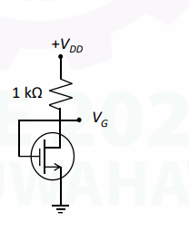
- A semiconductor uses P-type substrates with $N_A = 5 \times 10^{15}cm^{-3}$ in an n-MOS device having depletion region width of 0.415 $\mu$m. What is the depletion charge in magnitude?
- MOSFETs exhibit a non-linear relationship between input voltage and output current due to the device construction. The non-linear relationship is connected through the device parameter 'K'. Calculate 'K' for a specific MOSFET operating with an input voltage of 6 V and output current of 10 mA. The Threshold voltage of the chosen MOSFET is 4 V.
- What are the effects of increasing temperature in the I-V characteristics of the NMOS transistor ?
MOSFET can be used as a ____________.