
For the circuit shown in the figure, the delay of the bubbled NAND gate is 2 ns and that of the counter is assumed to be zero. If the clock (Clk) frequency is 1 GHz, then the counter behaves as a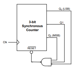
To determine the behavior of the counter in the given circuit, we need to analyze the setup shown in the figure.
The circuit consists of a 3-bit synchronous counter with outputs \(Q_0\), \(Q_1\), and \(Q_2\). There is a bubbled NAND gate used for resetting the counter, and its delay is given as 2 ns.
Let's analyze the counter's behavior step-by-step:
- The 3-bit counter can count from \(000_2\) to \(111_2\). Thus, it has a maximum count of \(2^3 = 8\) states.
- The bubbled NAND gate is used for resetting the counter when it reaches a specific count. It typically resets the counter when all outputs are high, i.e., \(111_2\).
- The counter theoretically counts up to 7 (binary 111) and then resets, hence completing a cycle or modulus operation.
- Given the clock frequency of 1 GHz, each clock cycle is 1 ns. However, the delay of the bubbled NAND gate is not sufficient to affect the counting because the counter's reset is in response to the counter state, not the clock.
Given these steps, the counter completes a full cycle by counting from 000 to 111 and then resets. Therefore, it behaves as a mod-8 counter since it counts 8 unique states including 000.
Thus, the correct answer is:
mod-8 counter
Important Questions from Counter
Which is not related to the counter circuit design?
A 16-bit synchronous binary up-counter is clocked with a frequency fCLK. The two most significant bits are OR-ed together to form an output Y. Measurements show that Y is periodic, and the duration for which Y remains high in each period is 24 ms. The clock frequency fCLK is ______ MHz. (Round off 2 decimal places.)
A MOD 2 and a MOD 5 up-counter when cascaded together results in a MOD ______ counter. (in integer)
A modulus 10 counter must have
How many flip-flops circuits are needed for a 4 bit counter?


