Arrange the following amplifiers in the order of maximum achievable voltage gain. Assume the geometry and overdrive voltage is same for the transistor M1 in all the circuits and $R_D < <r_{o1}$. choose the correct answer from the options given below: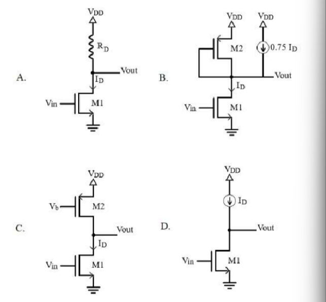
To determine the order of maximum achievable voltage gain for the given amplifiers, we need to analyze the gain configurations.
The voltage gain (\(A_v\)) of each amplifier configuration can be determined using the small-signal model for MOSFETs, considering parameters such as drain resistance and transconductance (\(g_m\)).
- Circuit A: Common Source (CS) with a resistor load.
- The voltage gain \(A_v\) is given by: \(A_v = -g_m R_D\).
- Where \(g_m\) is the transconductance and \(R_D\) is the load resistance.
- Circuit B: Common Source (CS) with a current mirror load.
- Due to the cascode effect and current mirror, the gain increases.
- Voltage gain \(A_v\) is approximately: \(A_v \approx -g_m r_{o1}\) (where \(r_{o1}\) is much larger).
- Circuit C: Cascode Configuration.
- This configuration boosts the output resistance significantly.
- Voltage gain \(A_v\) is given by: \(A_v \approx -g_m \cdot g_{m2} \cdot r_{o1} \cdot r_{o2}\) (very high gain).
- Circuit D: Common Source (CS) with an ideal current source load.
- The voltage gain approximates to the intrinsic gain of the MOSFET:
- \(A_v \approx -g_m r_{o1}\).
Based on the analysis, the circuits are in increasing order of voltage gain as follows:
- A : Moderate gain due to resistor load.
- B : Higher gain with current mirror providing increased output resistance.
- C : Highest gain due to the cascode effect increasing output resistance and gain.
- D : Comparatively lower gain with an ideal current source load.
Thus, the correct order is: A, B, C, D.
Important Questions from Feedback Amplifier
Arrange the following amplifiers in the order of maximum achievable -3dB frequency. Assume the transconductance ($g_m$) of the driver transistor (M1) same in all the circuits.
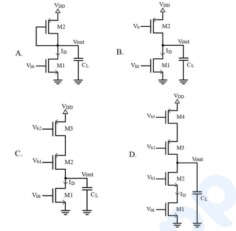
Choose the correct answer from the options given below:
The voltage gain of a certain amplifier without feedback is 10. With feedback its voltage gain reduces to 5. Determine its feedback factor.
Match the following lists :
List – I List – II a. Voltage series feedback i. Trans resistance amplifier b. Current series feedback ii. Current shunt feedback c. Current amplifier iii. Trans-conductance d. Voltage shunt feedback iv. Voltage amplifier Codes :
Match the following :
List – I List – II a. voltage shunt negative feedback i. increase of CMRR b. constant current source differential amplifier ii. O/P voltage attenuated by a factor 1/29 c. Phase shift oscillator iii. FSK decoder d. PLL iv. decrease of O/P impedance Codes :
Negative feedback in amplifier results in
1. reduced voltage gain
2. reduced bandwidth
3. increased S/N ratio
4. reduced distortion