
In the circuit below, assume that the long channel NMOS transistor is biased in saturation. The small signal trans-conductance of the transistor is $g_m$ . Neglect body effect, channel length modulation and intrinsic device capacitances. The small signal input impedance $Z_{in}(j\omega)$ is ________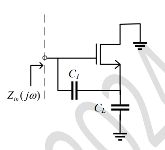
The given problem involves calculating the small signal input impedance \(Z_{in}(j\omega)\) in an NMOS transistor circuit with capacitors \(C_1\) and \(C_L\). The NMOS transistor is in saturation, and we need to find the equivalent impedance considering the trans-conductance \(g_m\).
Let's analyze the circuit step-by-step:
- The impedance of a capacitor in the frequency domain is given by \(Z_C = \frac{1}{j\omega C}\). Therefore, for capacitors \(C_1\) and \(C_L\), their impedances are \(\frac{1}{j\omega C_1}\) and \(\frac{1}{j\omega C_L}\) respectively.
- The controlled trans-conductance source due to \(g_m\) inverts the voltage, hence can be represented as a negative impedance which affects the input impedance at \(Z_{in}\).
- The effective input impedance \(Z_{in}(j\omega)\) can be derived by combining these impedances:
- The series combination of \(C_1\) and \(C_L\) results in an effective impedance of \(\frac{1}{j\omega C_1} + \frac{1}{j\omega C_L}\).
- The negative impact of the trans-conductance is given by \(-\frac{g_m}{C_1 C_L \omega^2}\), which arises from the feedback through the transistor.
- By summing these impedances, the expression for \(Z_{in}(j\omega)\) becomes:
\(Z_{in}(j\omega) = -\frac{g_m}{C_1 C_L \omega^2} + \frac{1}{j\omega C_1} + \frac{1}{j\omega C_L}\)
This matches the given correct answer option: \(-\frac{g_m}{C_1C_L\omega^2} + \frac{1}{j\omega C_1} + \frac{1}{j\omega C_L}\).
Figure: Circuit used for analysis
Important Questions from MOSFET
Which industry does aluminium smelting belong to?
Given, Vgs is the gate-source voltage, Vds is the drain source voltage, and Vth is the threshold voltage of an enhancement type NMOS transistor, the conditions for transistor to be biased in saturation are
A switched mode power supply operating at 20 kHz to 100 kHz range uses as the main switching element is __________.
Which semiconductor power device out of the following, is not a current triggering device?
A CMOS amplifier when compared to an N–channel MOSFET, has the advantage of


