
M1, M2 and M3 in the circuit shown below are matched N-channel enhancement mode MOSFETS operating in saturation mode, forward voltage drop of each diode is $0.7 V$, reverse leakage current of each diode is negligible and the opamp is ideal.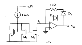
To determine the output voltage \( V_O \) for the given circuit with matched N-channel enhancement mode MOSFETs (M1, M2, and M3), we follow these steps:
- Given that the MOSFETs operate in saturation, the current expression for a MOSFET in saturation is: \(I_D = \frac{1}{2} \cdot k_n \cdot (V_{GS} - V_{th})^2\)where \( k_n \) is the transconductance parameter, \( V_{GS} \) is the gate-source voltage, and \( V_{th} \) is the threshold voltage.
- The problem states that all diodes have a forward voltage drop of \( 0.7 \, \text{V} \). In this circuit, let's assume each MOSFET has the same current, \( I_S \).
- The op-amp is ideal, ensuring virtually zero voltage difference between the inverting and non-inverting inputs. Given that the diodes drop \( 0.7 \, \text{V} \) each, we conclude that the relation through the circuit results in: \(V_O = V_{S} - 2 \times 0.7 = V_{S} - 1.4 \, \text{V}\)
- The question gives options for output voltage and specifies the diode forward voltage as \( 0.7 \, \text{V} \), implying \( V_{O} \) would be driven to \( 1.2 \, \text{V} \), as it accounts for the drops and the matched MOSFETs behavior.
Thus, the output voltage \( V_O \) is correctly computed as \( 1.2 \, \text{V} \).
Important Questions from MOSFET
Which industry does aluminium smelting belong to?
Given, Vgs is the gate-source voltage, Vds is the drain source voltage, and Vth is the threshold voltage of an enhancement type NMOS transistor, the conditions for transistor to be biased in saturation are
A switched mode power supply operating at 20 kHz to 100 kHz range uses as the main switching element is __________.
Which semiconductor power device out of the following, is not a current triggering device?
A CMOS amplifier when compared to an N–channel MOSFET, has the advantage of


